Principal Investigators: E. Deleporte (ENS Paris Saclay); C. Mayer(UVSQ)
Context and motivations
Recently the Hybrid Organic Perovskites HOP of chemical formula CH3NH3PbX3 (called 3D HOPs) represent a “material breakthrough”, particularly for photovoltaics: in only 3 years, the efficiency of HOP based solar cells has progressed from 12% to 22,7%, but also for light emitting devices: Amplified Spontaneous Emission (ASE) in HOP thin layers is demonstrated at room temperature, opening the way to HOP-based lasers and even to electrically injected lasers due to the good transport properties of this material. These HOPs are considered as a new class of semiconductors having amazing properties (good transport properties, high absorption coefficient) but still to explore. The team has a 13-year experience on the optical properties of HOPs and of photonic crystals such as vertical microcavities containing these HOPs. The team has obtained recently the laser effects in such cavities. The materials and the cavities are studied by means of micro-photoluminescence (PL), time-resolved PL, PL excitation, femtosecond pump-probe spectroscopy, as function of temperature.
Project
The project of the team centered will be developed according to three main topics:
- Development and optical investigation of new HOP monocrystalline thin films (D. Garrot & E. Deleporte)
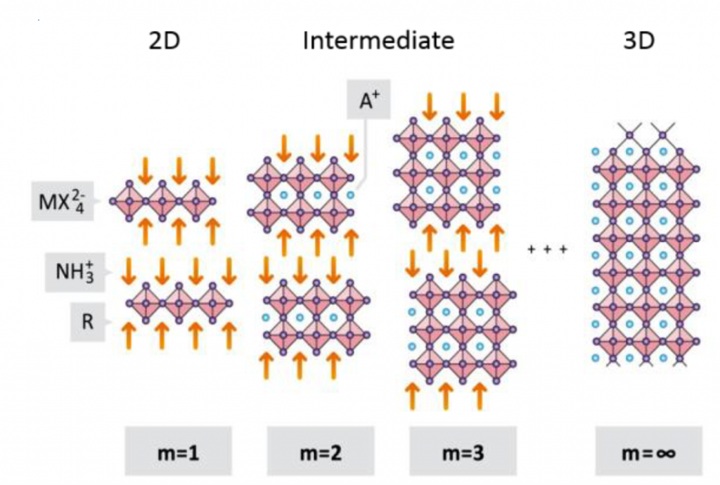
The 3D HOPs are sensitive to moisture, their stability is then a main technological issue to overcome. The solution might come from HOPs of formula (ANH3)2(CH3NH3)m-1PbmX3m+1 (A: organic group, X: halogen). The variable m corresponds to the number of inorganic layers intercalated between the organic molecules: for m=1, the material is a 2D perovskite, where carriers are confined in an atomically thin inorganic layer, made of PbX6 octahedrons, and form strongly bound excitons (Figure 9). At the limit case of m=∞, we obtain the 3D hybrid perovskite CH3NH3PbX3 for which the exciton binding energy is only of a few meV and the transport properties are dominated by free carriers at room temperature. From m=1 (2D) to m=∞ (3D), the dimensionality, and thus the excitonic properties of HOPs, can be tailored. Nevertheless, the charge carrier properties of these HOPs are largely unknown for the moment. Contrary to standard quantum wells, the high contrast between the dielectric constants of the organic and inorganic part generates a dielectric confinement of the carriers, making the physics of the excitons more complex. Besides, Coulombic interaction between the carriers and the dipole moment of the organic cation (A+: CH3NH2+) lead to the formation of specific polaronic states. In order to study the intrinsic properties of these new HOPs and to produce high crystallinity thin layers integrable in devices, we will grow monocrystalline thin films HOPs, presenting pure phase (crystals in which a single m is present) exhibiting a high aspect ratio aspect (thickness from 100 nm to several 100 nm, surface of cm2), using a crystallization method developed recently in our group (the Anti-Solvent Vapor-assisted Capping Crystallization).
- Laser effect in microcavities containing hybrid perovskites (E. Deleporte & D. Garrot)
Performances of the HOP-based opto-electronic devices are currently limited by the low crystallinity of the thin HOP layers which affects drastically the exciton diffusion lengths and the carriers’ mobility. So, in a first step, we will realize microcavities containing these new HOPs thin monocrystalline layers as the active material and study their emission properties with pulsed and continuous optical excitation in cavity: exciton-polaritons in strong coupling cavities, lasing. In a second step, we will explore the possibility to realize an injected compact solid state laser source in collaboration with INL Lyon and XLIM Limoges.
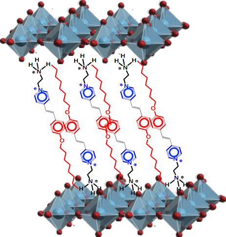
- Design of new organic chromophores to realize 2D and Nanometic Hybrid Perovskite Materials (C. Mayer). By this molecular engineering, we target either emissive or photo-diodes materials, for visible light communication application (so-called LiFi technology or VLC). To date, VLC is an emerging field because it allows sending digital data by modulating LED light, without radio waves. However, if, with a conventional lighting, it’s possible to send a signal up to 500 Mbit/s, a current smartphone can neither receive nor send an equivalent signal by VLC. In addition, given the emergence of organic electronics, smartphones are becoming thinner and more foldable, that means the use of more and more conformable electronic components. The objective of this axis is to design a whole molecular engineering around 2D / Nano Hybrid Perovskite Materials to control and optimize the photonic emission and reception properties of these materials. This control is done by integrating organic luminophores with modular emission wavelengths in the organic part of the perovskites. It’s the contribution of soft chemistry that allowing fine-tuning of the structure of these materials and their HOMO-LUMO energy gap, leading to innovative photonic materials.